Module axi_interconnect
This document contains technical documentation for the axi_interconnect module.
An AXI interconnect is a glue logic box that instantiates a combination of
AXI data width converter,
AXI clock domain crossing,
AXI data FIFO,
AXI read/write throttling,
AXI crossbar
for each port depending on it’s attributes.
The goal of this AXI interconnect implementation developed by Truestream is to deliver 100% throughput in all scenarios. This means never stalling the data bus by even a single cycle, even if the user application is not always well-behaved in an AXI sense.
Examples
Example with left-side processing
Below is an illustration of a few scenarios with processing on the left side of the crossbar.
This is the typical use case, and in this scenario the interconnect guarantees 100% throughput
to the right side.
![digraph my_graph {
graph [ dpi = 300 splines=ortho];
rankdir="LR";
left_port_0 [ shape=none label="Left port 0:\n64 bit\n100 MHz\nwell-behaved" ];
axi_cdc_0 [ shape=box label="AXI CDC"];
axi_write_throttle_0 [ shape=box label="AXI write\nthrottle"];
left_port_0 -> axi_cdc_0 [ dir="none" weight=10 ];
axi_cdc_0 -> axi_write_throttle_0 [ dir="none" weight=10 ];
left_port_1 [ shape=none label="Left port 1:\n128 bit\n100 MHz\nwell-behaved" ];
axi_cdc_1 [ shape=box label="AXI CDC"];
axi_data_width_converter_1 [ shape=box label="AXI data\nwidth converter"];
left_port_1 -> axi_cdc_1 [ dir="none" ];
axi_cdc_1 -> axi_data_width_converter_1 [ dir="none" weight=10 ];
left_port_2 [ shape=none label="Left port 2:\n128 bit\n250 MHz\nill-behaved" ];
axi_data_width_converter_2 [ shape=box label="AXI data\nwidth converter"];
axi_cdc_2 [ shape=box label="AXI CDC"];
axi_write_throttle_2 [ shape=box label="AXI write\nthrottle"];
left_port_2 -> axi_data_width_converter_2 [ dir="none" ];
axi_data_width_converter_2 -> axi_cdc_2 [ dir="none" weight=10 ];
axi_cdc_2 -> axi_write_throttle_2 [ dir="none" weight=10 ];
left_port_3 [ shape=none label="" ];
dots_3 [ shape=none label=".\n.\n." ];
left_port_3 -> dots_3 [ style=invis weight=10 ];
{
rank=same; left_port_0; left_port_1; left_port_2; left_port_3;
}
{
rank=same; dots_3; axi_cdc_2;
}
axi_write_crossbar [ shape=box label="AXI write\ncrossbar" height=4.4];
axi_write_throttle_0 -> axi_write_crossbar [ dir="none" ];
axi_data_width_converter_1 -> axi_write_crossbar [ dir="none" ];
axi_write_throttle_2 -> axi_write_crossbar [ dir="none" ];
dots_3 -> axi_write_crossbar [ style="invis" ]
right_port [ shape=none label="Right port:\nwell-behaved\n200 MHz\n64 bit" ];
axi_write_crossbar -> right_port [ dir="none" ];
}](../../_images/graphviz-af84404284ad82ad9cefeee8fc7426f3b369ef94.png)
The examples above instantiate different processing blocks depending on the configuration of the
left ports.
The processing blocks achieve the goal of ensuring the AXI transactions are well-behaved before
reaching the crossbar, so that no cycles are wasted on the right side.
The left port 0 has the same data width as the right port, but is in a different clock
domain, so it needs a clock crossing.
Since the clock rate is lower on the left side for this port the bus also needs to be throttled.
The clock crossing from 100 MHz to 200 MHz would otherwise yield a data word every second cycle in
the right domain.
For left port 1, the relation of clock rate and data width means the data rate is the same on
the left side and the right side.
This means that the transactions are still well-behaved when reaching the crossbar, given that they
are well-behaved from the AXI master on the left side.
Port 2 on the left is configured to indicate that the AXI master is not well-behaved.
In this case there is need for a throttling block, despite the data rate being high enough to send
with full throughput on the right side.
Since an ill-behaved AXI master might start sending a burst but pause halfway in, the throttle block
must buffer a full burst before sending it through to the crossbar.
Example with right-side processing
It is also possible to place processing blocks on the right side of the crossbar.
This can be suitable in a few scenarios.
For example:
![digraph my_graph {
graph [ dpi = 300 splines=ortho];
rankdir="LR";
left_port_0 [ shape=none label="Left port 0:\n64 bit\n300 MHz\nwell-behaved" ];
left_port_1 [ shape=none label="Left port 1:\n128 bit\n300 MHz\nwell-behaved" ];
axi_data_width_converter_1 [ shape=box label="AXI data\nwidth converter"];
left_port_1 -> axi_data_width_converter_1 [ dir="none" weight=10 ];
{
rank=same; left_port_0; left_port_1;
}
axi_write_crossbar [ shape=box label="AXI write\ncrossbar" height=2.5];
left_port_0 -> axi_write_crossbar [ dir="none" ];
axi_data_width_converter_1 -> axi_write_crossbar [ dir="none" ];
axi_cdc_right [ shape=box label="AXI CDC"];
right_port [ shape=none label="Right port:\nwell-behaved\n250 MHz\n64 bit" ];
axi_write_crossbar -> axi_cdc_right [ dir="none" ];
axi_cdc_right -> right_port [ dir="none" ];
}](../../_images/graphviz-eab0cf6c9897332edc63843e29a9af6d5cbebda7.png)
In this case both of the left ports are in the same clock domain, and the right port is in
a slower domain.
This means it is more efficient to run the crossbar in the left clock domain, and have only one
CDC on the right side.
Warning
Placing processing blocks after the crossbar is considered a niche use-case, and the interconnect can not guarantee 100% utilization in all scenarios.
Specifically an AXI data width converter can be placed after the crossbar, which will
have a one clock cycle overhead per burst. In that case the throughput on the right will not
be 100% even if the left ports push data at a high enough rate.
In others scenarios, such as the one illustrated above, it is however completely safe to place processing blocks after the crossbar.
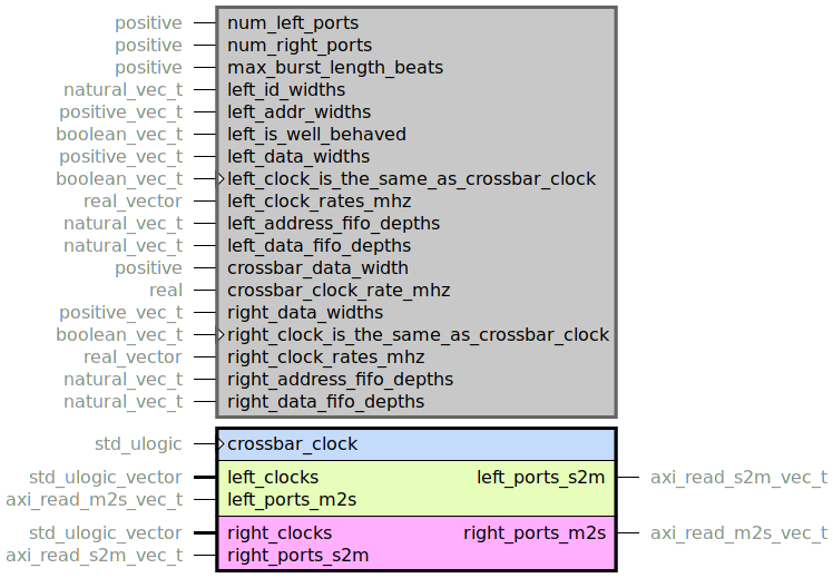
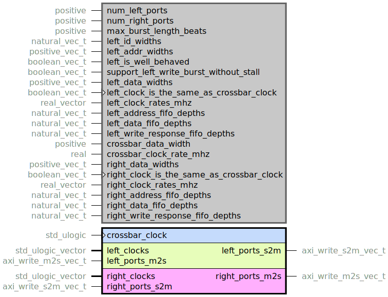
Configuration interface
The properties of the left and right ports are set via generics to
axi_read_interconnect and
axi_write_interconnect.
The following generics are available:
num_left_ports: The number of ports on theleftside.num_right_ports: The number of ports on therightside. Must be set to one.max_burst_length_beats: The maximum AXI burst length to be used. Typically set to 16 or 256.left_id_widths: The AXI ID width used for each port on theleftside. A higher value will result in greater resource utilization.Note that the AXI ID width used on the
rightside will be the maximum ofleft_id_widthsplus some spare bits used for response arbitration. See documentation ofaxi_crossbar.left_addr_widths: The AXI address width used for each port on theleftside. A higher value will result in greater resource utilization.Note that the AXI address width used on the
rightside will be the maximum ofleft_addr_widths.left_is_well_behaved: Set totrueif the AXI master to theleftis guaranteed to be well-behaved. One value for each port.Setting a value of
falsemight necessitate the insertion of AXI FIFOs and/or throttling blocks, which will increase the resource utilization.left_data_widths: The AXI data width used for each port on theleftside.left_clock_is_the_same_as_crossbar_clock: Set totrueif theleftport AXI clock is the same as thecrossbar_clockport. One value for eachleftport.A value of
falsewill necessitate the insertion of AXI CDCs before the crossbar.left_clock_rates_mhz: The clock rate in MHz for each port on theleft. The clock and data rate configuration will in some cases determine the need for buffering and throttling.left_address_fifo_depths: In cases where FIFO buffering is instantiated before the crossbar, this generic controls the depths of the address (AR/AW) FIFOs. One value per port.Note that the value zero can be set to generate a passthrough instead of a FIFO.
left_data_fifo_depths: In cases where FIFO buffering is instantiated before the crossbar, this generic controls the depths of the data (R/W) FIFOs. One value per port. To guarantee full throughput, a value of at leastmax_burst_length_beatsmust be used.Note that the value zero can be set to generate a passthrough instead of a FIFO.
crossbar_data_width: The AXI data width used by the crossbar.Note that a different value than
left_data_widthsfor any given port will insert a data width converter for that port before the crossbar. A different value thanright_data_widthswill insert data width conversion after the crossbar.crossbar_clock_rate_mhz: The clock rate in MHz for thecrossbar_clockport.Note that if this value is different than
left/right_clock_rate_mhzfor any given port, thenleft/right_clock_is_the_same_as_crossbar_clockmust be set tofalse. Conversely ifleft/right_clock_is_the_same_as_crossbar_clockistruethenleft/right_clock_rates_mhzmust be the same ascrossbar_clock_rate_mhzfor that port.Having the same
*_clock_rate_mhzvalue butleft/right_clock_is_the_same_as_crossbar_clockset tofalseis valid in situations where two clocks have the same frequency but come from different clocks sources. This situation necessitates the insertion of CDCs despite the clocks having the same frequency.right_data_widths: The AXI data width used for each port on therightside.A value different than
crossbar_data_widthwill necessitate insertion of data width conversion after the crossbar.right_clock_is_the_same_as_crossbar_clock: Set totrueif therightport AXI clock is the same as thecrossbar_clockport. One value for eachrightport.A value of
falsewill necessitate the insertion of AXI CDCs after the crossbar.right_clock_rates_mhz: The clock rate in MHz for each port on theright. The clock and data rate configuration will in some cases determine the need for buffering and throttling.right_address_fifo_depths: In cases where FIFO buffering is instantiated after the crossbar, this generic controls the depths of the address (AR/AW) FIFOs. One value per port.Note that the value zero can be set to generate a passthrough instead of a FIFO.
right_data_fifo_depths: In cases where FIFO buffering is instantiated after the crossbar, this generic controls the depths of the data (R/W) FIFOs. One value per port. To guarantee full throughput, a value of at leastmax_burst_length_beatsmust be used.Note that the value zero can be set to generate a passthrough instead of a FIFO.
Additionally axi_write_interconnect has the generics:
support_left_write_burst_without_stall: Set totruein order to ensure there is buffering on theleftside that can receive a whole data burst without stalling. See more under Left write bursts without stall.Setting a value of
truemight necessitate the insertion of AXI FIFOs and/or switch the order of processing blocks, which will increase the resource utilization.left_write_response_fifo_depths: In cases where FIFO buffering is instantiated before the crossbar, this generic controls the depths of the write response (B) FIFOs. One value per port.Note that the value zero can be set to generate a passthrough instead of a FIFO.
right_write_response_fifo_depths: In cases where FIFO buffering is instantiated after the crossbar, this generic controls the depths of the write response (B) FIFOs. One value per port.Note that the value zero can be set to generate a passthrough instead of a FIFO.
Left write bursts without stall
There is a configuration option to support left-side write bursting without stall for each port.
If any AXI master on the left is written in such a way that it is important for it to send
bursts of data without stall, then this option must be considered.
If on the other hand it is not important for the AXI master, or bursted data is buffered in a
FIFO already, then this option can be set to false to save resources.
The use case for this is somewhat convoluted but consider the following processing chain:
![digraph my_graph {
graph [ dpi = 300 splines=ortho];
rankdir="LR";
left_port [ shape=none label="64 bit\n300 MHz\nill-behaved" ];
axi_data_width_converter [ shape=box label="AXI data\nwidth converter"];
axi_cdc [ shape=box label="AXI CDC"];
axi_write_throttle [ shape=box label="AXI write\nthrottle"];
right_port [ shape=none label="32 bit\n250 MHz\nwell-behaved" ];
left_port -> axi_data_width_converter [ dir="none" ];
axi_data_width_converter -> axi_cdc [ dir="none" ];
axi_cdc -> axi_write_throttle [ dir="none" ];
axi_write_throttle -> right_port [ dir="none" ];
}](../../_images/graphviz-da1d3ffb06080dead04a1949954df2d8f2402e72.png)
In this case there is full throughput on the right side, but the left side can only do a data
transaction every second cycle due to the width conversion from 64 to 32.
If we were to set the support_left_write_burst_without_stall generic to true for this port,
the processing blocks would be re-ordered to this configuration:
![digraph my_graph {
graph [ dpi = 300 splines=ortho];
rankdir="LR";
left_port [ shape=none label="64 bit\n300 MHz\nill-behaved" ];
axi_cdc [ shape=box label="AXI CDC"];
axi_write_throttle [ shape=box label="AXI write\nthrottle"];
axi_data_width_converter [ shape=box label="AXI data\nwidth converter"];
right_port [ shape=none label="32 bit\n250 MHz\nwell-behaved" ];
left_port -> axi_cdc [ dir="none" ];
axi_cdc -> axi_write_throttle [ dir="none" ];
axi_write_throttle -> axi_data_width_converter [ dir="none" ];
axi_data_width_converter -> right_port [ dir="none" ];
}](../../_images/graphviz-95e1774f01a9743d9cad6605c13c2e850842a17a.png)
With the AXI CDC being placed first in the chain, the AXI master to the left can burst to
the CDC data FIFO without stalling.
The downside of this configuration is that the AXI CDC will have a little higher resource
utilization when it is placed on a wider bus.
AXI well-behavedness
The concept of an AXI master/slave being well-behaved is recurring in the discussion of this module. For an AXI participant to be considered well-behaved it has to fulfill some requirements. First of all, the AXI standard AMBA AXI and ACE Protocol Specification, ARM IHI 0022E (ID022613) must be followed. Secondly, the general rules of handshaking data interfaces must be followed. And apart from that, there are some specific requirements depending on what actor we are discussing, listed below.
AXI read master
An AXI read master must adhere to the following requirements to be considered well-behaved.
The
RREADYsignal must be asserted in the same cycle, or before, the correspondingARVALID.I.e. a master shall not negotiate a burst, but not be able to receive the data.
Once
RREADYhas been asserted, it must remain high until theRLASTtransaction has occurred.I.e. there must never be holes in the data stream. This will unnecessarily stall the AXI slave and decrease bus utilization.
AXI read slave
An AXI read slave must adhere to the following requirements to be considered well-behaved.
When
ARREADYhas been asserted the slave should be ready to assertRVALIDas soon as possible.The AXI master might have a state machine that waits to receive data before it can continue processing.
Once
RVALIDhas been asserted, it must remain high until theRLASTtransaction has occurred.I.e. there must never be holes in the data stream. This will unnecessarily stall the AXI master and decrease bus utilization.
AXI write master
An AXI write master must adhere to the following requirements to be considered well-behaved.
The
WVALIDsignal must be asserted in the same cycle, or before, the correspondingAWVALID.I.e. a master shall not send it’s address transaction, and then wait a long while before starting to send data. Sending the data before the address is acceptable though.
If
WVALIDis asserted before it’s correspondingAWVALID, no more than one burst of data shall be sent before the address transaction is sent.I.e. a master shall not fill up the data buffering with data, but the address transaction necessary to interpret the data comes way later.
Once
WVALIDhas been asserted, it must remain high until theWLASTtransaction has occurred.I.e. there must never be holes in the data stream. This will unnecessarily stall the AXI slave and decrease bus utilization.
The
BREADYsignal must be constantly asserted.I.e. the master must always be able to receive the write response. Stalling the write response channel can fill the response queue of the AXI slave, which in turn stalls
AWandWtransactions.
AXI write slave
An AXI write slave must adhere to the following requirements to be considered well-behaved.
Once
AWREADYis asserted the slave must within a few clock cycles assertWREADY.Having
WREADYasserted beforeAWREADYis also acceptable.Accepting address transactions but not being able to accept data can stall an AXI master.
Once
WREADYhas been asserted, it must remain high until theWLASTtransaction has occurred.I.e. there shall never be holes in the data stream. This will unnecessarily stall the AXI master and decrease bus utilization.
The write response shall be sent as soon as possible.
The AXI master might have state machine that waits for a write response before it can continue processing.
Handshaking rules
The AXI interfaces used by this module feature handshaking via ready/valid.
Using AXI4-Stream-like handshake interfaces (ready and valid to qualify data transactions)
is very common in FPGA designs.
It enables a backpressure situation where the slave, i.e. the receiver of data, can indicate when it
is ready to receive the data.
Below are some rules governing how these handshake signals interact. They are adapted from the AMBA 4 AXI4-Stream Protocol Specification, ARM IHI 0051A (ID030610).
A transactions occurs on the positive edge of the clock when both
readyandvalidare high. The graph below shows some typical transactions.
The
readysignal may fall without a transaction having occurred:
The
validsignal may NOT fall without a transaction having occurred:
Once
validis asserted, the associated data may NOT be changed unless a transaction has occurred.
This applies to any auxillary signals associated with the bus as well, e.g. a
lastindicator.Note also that this restriction on data not changing only applies when
validis asserted. When it is not, the data may be changed freely.In order to avoid deadlock situations, the master may NOT wait for the slave to assert
readybefore assertingvalid. The slave however may wait forvalidbefore assertingready.
axi_interconnect_pkg.vhd
Package with types and utility functions for this module.
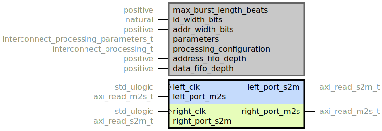
axi_read_interconnect.vhd
Top level for AXI read interconnect that instantiates processing before and after the crossbar based on the generic configuration set by the user.
Resource utilization
This entity has netlist builds set up with
automatic size checkers
in module_axi_interconnect.py.
The following table lists the resource utilization for the entity, depending on
generic configuration.
Generics |
Total LUTs |
FFs |
RAMB36 |
RAMB18 |
|---|---|---|---|---|
num_left_ports = 4 num_right_ports = 1 (Using wrapper axi_read_interconnect_netlist_wrapper.vhd) |
1090 |
1622 |
4 |
0 |
axi_write_interconnect.vhd
Top level for AXI write interconnect that instantiates processing before and after the crossbar based on the generic configuration set by the user.
Resource utilization
This entity has netlist builds set up with
automatic size checkers
in module_axi_interconnect.py.
The following table lists the resource utilization for the entity, depending on
generic configuration.
Generics |
Total LUTs |
FFs |
RAMB36 |
RAMB18 |
|---|---|---|---|---|
num_left_ports = 4 num_right_ports = 1 (Using wrapper axi_write_interconnect_netlist_wrapper.vhd) |
1418 |
1728 |
4 |
4 |
read_interconnect_processing.vhd
Utility box that instantiates a chain of processing boxes based on a configuration vector.
write_interconnect_processing.vhd
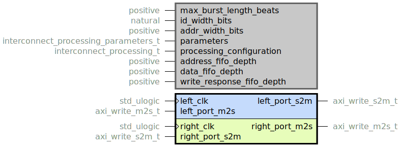
Utility box that instantiates a chain of processing boxes based on a configuration vector.
Resource utilization
This entity has netlist builds set up with
automatic size checkers
in module_axi_interconnect.py.
The following table lists the resource utilization for the entity, depending on
generic configuration.
Generics |
Total LUTs |
FFs |
RAMB36 |
RAMB18 |
|---|---|---|---|---|
support_left_write_burst_without_stall = False (Using wrapper write_interconnect_processing_netlist_wrapper.vhd) |
357 |
568 |
1 |
1 |
support_left_write_burst_without_stall = True (Using wrapper write_interconnect_processing_netlist_wrapper.vhd) |
361 |
568 |
2 |
1 |